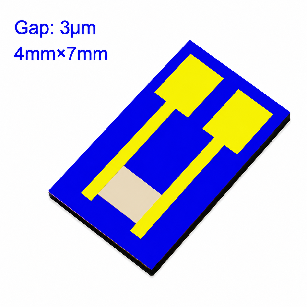
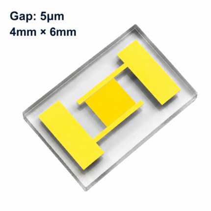
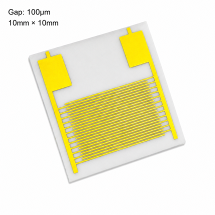
EAP1 3μm Silicon-Based Interdigitated Electrode (IDE) Capacitive Array for MEMS Gas and Biosensors, Electrochemical and Photoelectric Detection

$35.00

Size

Default

SKU: EAP1 Category:
Description
Potentiolab • Silicon-Based Interdigitated Electrode

3μm Silicon-Based Interdigitated Electrode MEMS Sensor Chip

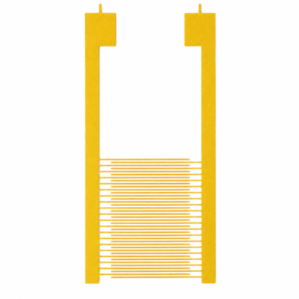
Ultra-fine 3μm silicon-based interdigitated electrode designed for MEMS gas, humidity, biological, chemical, physical, and medical sensor chip applications with high precision and stable sensing performance.

3μm IDE GapSingle-Crystal Silicon

Ti/Au Electrode

3 micron silicon based interdigitated electrode MEMS gas humidity biosensor chip
ultra fine silicon based interdigitated electrode capacitive array for MEMS gas and biological sensing
Ultra-Fine IDE Structure
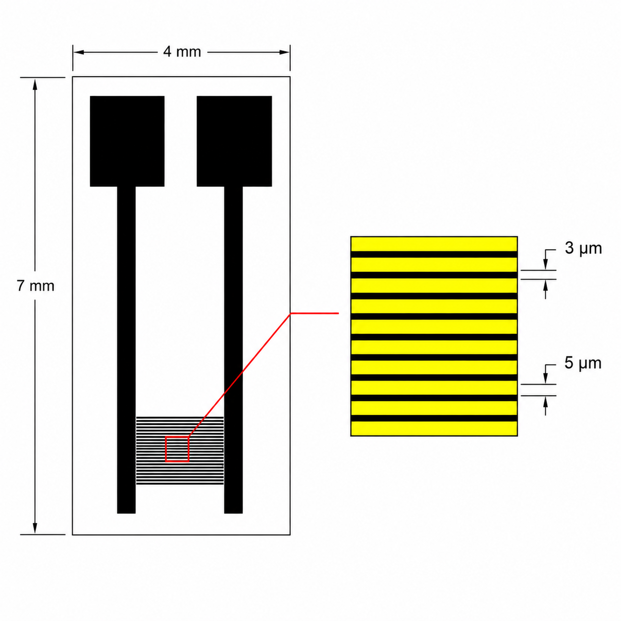
  • Line width: 5μm
  • Line spacing: 3μm
  • Finger length: 1.6mm
  • 75 pairs / 150 fingers
Single-Crystal Silicon Substrate
  • Single-crystal silicon substrate
  • Surface-grown SiO₂ insulating layer
  • SiO₂ thickness: 300nm
  • Suitable for MEMS sensor integration
Ti/Au Metal Layer
  • Metal layer structure: Ti/Au
  • Ti thickness: 30nm
  • Au thickness: 100nm
  • Excellent conductivity and stability
Wide Operating Temperature
  • Operating temperature: -150°C to 500°C
  • Excellent thermal stability
  • Reliable sensing performance
  • Suitable for harsh laboratory environments
Typical Applications
  • MEMS gas sensors
  • Humidity-sensitive sensors
  • Biological sensor chips
  • Chemical and physical sensors
  • Medical sensor research
ItemSpecification
Product Name3μm Silicon-Based Interdigitated Electrode MEMS Sensor Chip
Overall Size4mm × 7mm × 0.52mm
Line Width5μm
Line Spacing3μm
Finger Length1.6mm
Interdigitated Pairs75 pairs / 150 fingers
SubstrateSingle-crystal silicon
Insulating LayerSurface-grown SiO₂, 300nm
Metal Layer StructureTi/Au
Metal Layer ThicknessTi 30nm / Au 100nm
Operating Temperature-150°C to 500°C
Product Advantages
This ultra-fine silicon-based interdigitated electrode features a 3μm IDE gap structure, SiO₂-insulated single-crystal silicon substrate, and Ti/Au conductive layer system. It is suitable for MEMS gas, humidity, biological, chemical, physical, and medical sensing applications requiring high precision, reliable performance, and stable quality.
Precautions
  • Handle carefully to avoid scratching the electrode surface.
  • Avoid mechanical impact or excessive force on the silicon substrate.
  • Clean gently with suitable laboratory-grade solvents before use.
  • Store in a clean, dry, and dust-free environment.
  • Custom electrode dimensions and patterns are available upon request.
Reviews (0)

Reviews

There are no reviews yet.

Be the first to review “EAP1 3μm Silicon-Based Interdigitated Electrode (IDE) Capacitive Array for MEMS Gas and Biosensors, Electrochemical and Photoelectric Detection”

Your email address will not be published. Required fields are marked *

Shipping and Delivery

Worldwide Shipping

Potentiolab ships electrochemical electrodes, electrochemical cells, and laboratory accessories to universities, research institutes, and laboratories worldwide. Orders are shipped primarily via FedEx International Priority (occasionally DHL or UPS) with full tracking. In-stock items are typically dispatched within one business day. Estimated delivery times are 4–6 working days for Asia, 5–7 working days for Europe and North America, and 7–9 working days for other regions. Customs clearance times may vary by country.

Rates, Support & Orders

Shipping fees start from USD 28, with free shipping available on qualifying orders over USD 1800. Prices exclude VAT, customs duties, or local taxes, which are the responsibility of the recipient. For bulk orders, custom electrochemical products, academic discounts, or institutional purchasing requirements, please contact our sales team at sales@potentiolab.com.